How Is GaN-on-Diamond Made?
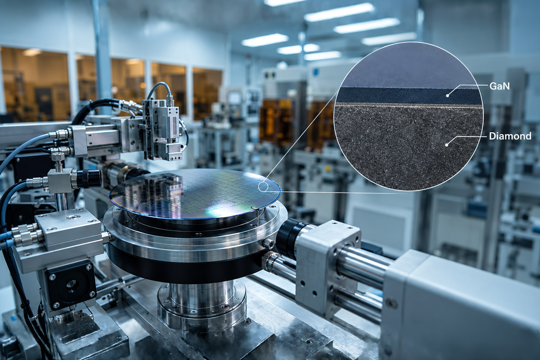
GaN (Gallium Nitride), a wide-bandgap semiconductor, has high electric-field strength and electron mobility. These properties have made GaN HEMTs ideal for radio-frequency communications and renewable energy generation. However, when it comes to high-power applications, HEMT devices are still thermally limited. The best solution here is to pair GaN with diamond, as it possesses the highest thermal conductivity. Since GaN and diamonds have different crystal structures and expand differently when heated, growing GaN directly on diamond becomes slightly difficult.
The manufacturing of GaN-on-Diamonds is undertaken via three different methods. In this blog, we'll explore the three main methods for manufacturing GaN-on-diamond.
About GaN-on-Diamond
GaN-on-Diamond technology is an approach wherein gallium nitride is combined with a diamond substrate. The result of this integration is better thermal conductivity and excellent efficiency, which makes it ideal for high-power applications.
Methods of Building GaN-on-Diamond
Since gallium nitride and diamonds have different crystal structures, growing GaN directly on diamond can be a challenge. To resolve this issue, there are three different methods to grow GaN on diamond, which are briefly discussed in this section:
1. Low-Temperature Wafer Bonding
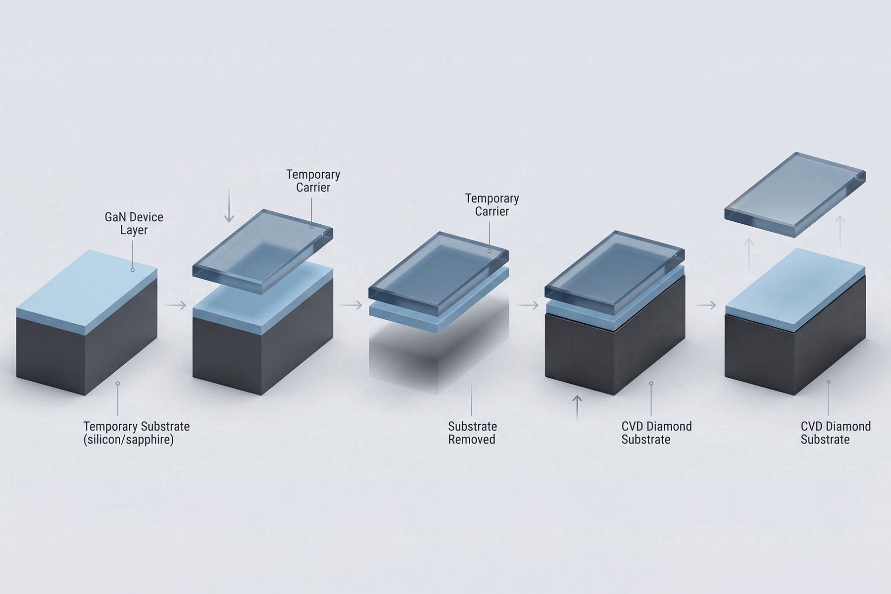
This low-temperature wafer bonding method is one in which a fully developed GaN device layer is joined with a separately prepared substrate of CVD diamond. According to this method, both diamond and GaN are produced separately. This helps prevent the high temperatures required in CVD diamond growth from damaging the GaN device layer.
Key Steps Involved
- Growing GaN: A temporary substrate, including silicon, sapphire, or silicon carbide, is used to grow the GaN device layer.
- Temporary Carrier Attachment: During the processing, the GaN wafer is attached to a glass or silicon carrier.
- Removing the Substrate: Later, the original substrate and unwanted layers are removed, which exposes a thin and clean GaN layer.
- Diamond Bonding: The key technology for this step is surface-activated bonding (SAB). Inside a vacuum chamber, the polished surfaces of the GaN layer and the diamond are cleaned at the atomic level using a beam of argon atoms. This removes oxides and contaminants and leaves highly reactive surfaces, which bond as soon as they are pressed together, at room temperature and without an adhesive layer.
- Carrier Removal: Finally, the temporary carrier is detached, and the thin GaN device layer is bonded to the diamond substrate.
With the low-temperature bonding of GaN with high-quality single-crystal diamond, a thermal conductivity of around 2000 W/m.K can be achieved. As the temperature stays below 400 degrees C, the stress is reduced, which helps prevent the GaN layer from cracking.
Importance of Surface-Activated Bonding
In 2021, the researchers at Osaka City University in Japan used SAB to bond GaN directly to a 10 × 10 mm diamond plate. The bond survived heating up to 1,000 °C without peeling, well above the 700 °C needed to make GaN devices. The heat even shrank the thin damaged layer at the interface from about 5.3 nm to 1.5 nm, as amorphous carbon there converted into diamond. The researchers report that the temperature rise in GaN transistors was suppressed by a factor of four.
2. CVD Diamond Growth on GaN
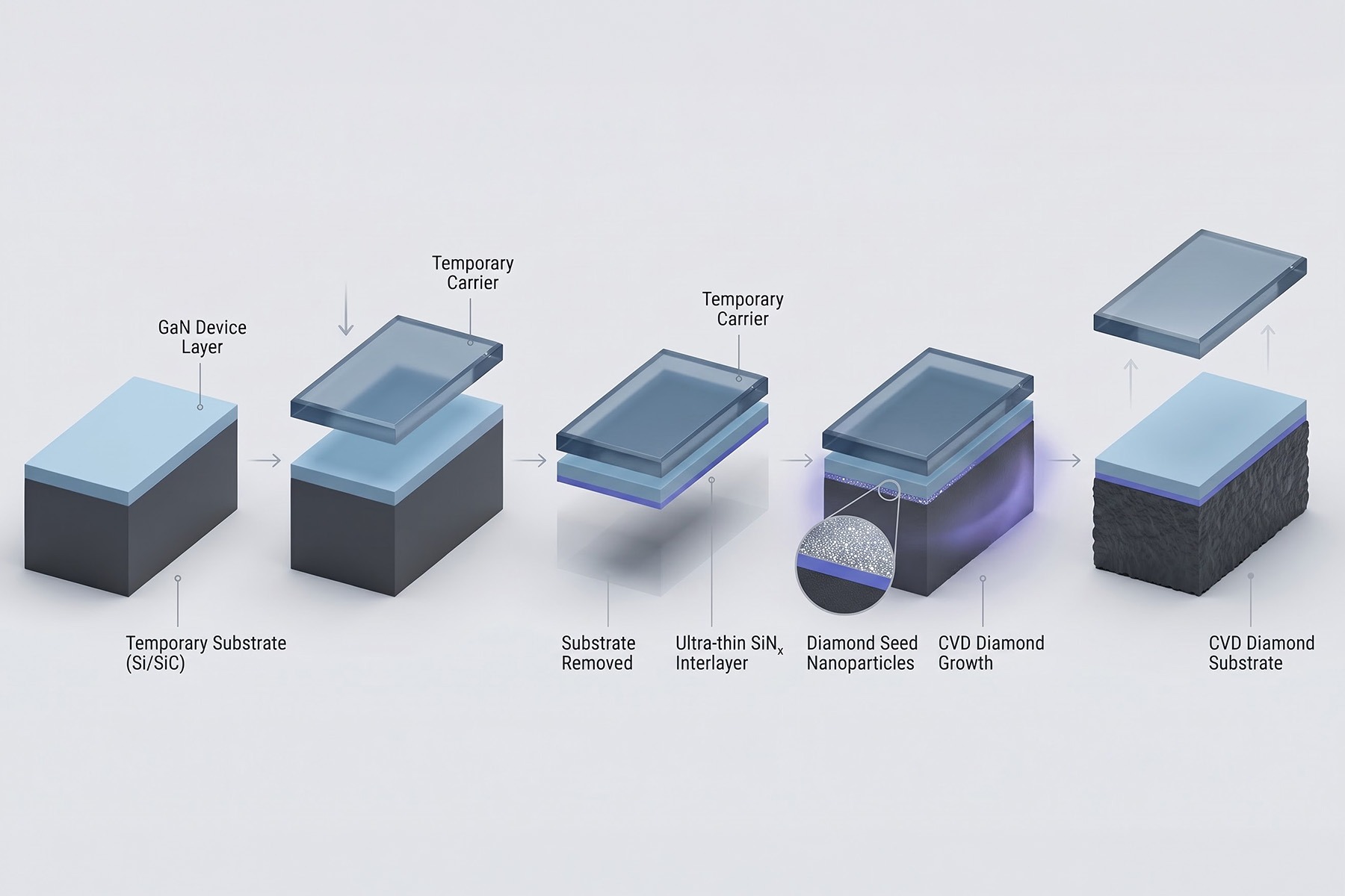
The second method for growing GaN-on-diamond is via a chemical vapor deposition growth process. Under this method, the diamond layer is grown onto the back of a thin GaN wafer. A separate diamond substrate is not attached in this case.
Key Steps Involved
a. Growing the GaN Device Structure
The GaN device layers are grown on a temporary substrate, usually silicon or silicon carbide.
b. Bonding the Wafer
The wafer is flipped, and the active side is attached to a temporary glass or silicon carrier via a suitable bonding layer. This carrier provides support to the delicate GaN structure.
c. Removing the Original Substrate
The original silicon or SiC substrate is removed from the backside by etching it away. This process removes the relevant transition layers during the GaN growth. This exposes the underlying GaN layer for the next stage.
d. Placing a Protective Layer
The growth of diamond requires hydrogen-rich plasma conditions that can cause damage to the exposed GaN. To protect GaN from this damage, an extremely thin dielectric interlayer of either silicon nitride (SiN) or aluminium nitride (AIN) is applied. This layer helps protect the GaN during the diamond synthesis process.
e. Seeding the Surface
The ready surface is then coated with tiny diamond particles, which are known as nanodiamonds. These nanodiamonds are the first step in the diamond growth process and help in the formation of a continuous film across the wafer.
f. The Diamond Layer
The wafer is grown in the Microwave Plasma Chemical Vapor Deposition (MPCVD) reactor, wherein a mixture of methane and hydrogen gases is activated by microwave energy.
As the process continues, the individual diamond crystals form a thick polycrystalline diamond layer, which helps move the heat away from the GaN device. Once the diamond is grown, the temporary carrier is removed.
The benefit of growing diamond directly on the GaN substrate is that it eliminates the need to attach a separately manufactured diamond plate. Group4 Labs, a US company, first made a GaN-on-diamond chip this way in 2006, and it is now the most commercially mature method.
The Future is Built At the Interface
To conclude, GaN-on-Diamond technology offers a promising solution to one of the biggest problems in modern electronics: managing heat. The excess amount of heat generated during operation impacts device performance. The high thermal conductivity of diamonds allows the heat to move away from the device efficiently.
The process of building GaN-on-diamond substrates is complicated. The different crystal structures and thermal expansion properties of GaN and diamond make it difficult to combine them directly. To overcome these challenges, there are 3 different approaches undertaken for growing GaN-on-Diamond.
However, despite these challenges, GaN-on-Diamond technology has proven to have significant potential in applications including 5G and 6G communication, radar systems, electric vehicles, and power electronics. As research and manufacturing techniques advance, the integration of GaN-on-Diamonds might get smoother in the future.
Frequently Asked Questions
Here are some frequently asked questions on how GaN-on-Diamond is built:
“redefining one diamond layer at a time”
More Articles



Aga9 Systems is a lab-grown diamond manufacturing company dedicated to harnessing the valuable properties of CVD diamonds for industrial applications. We at Aga9 Systems manufacture more than lab-grown diamond plates, we are dedicated to creating brilliance ethically, sustainably and with maximum resource efficiency.