GaN on Si vs GaN on SiC vs GaN on Diamond HEMT: Key Differences Explained

GaN offers several advantages including wide bandgap, high electron mobility and high breakdown field. Applications including RF communication, high-power electronics and aerospace systems have benefitted immensely with GaN HEMTs. As the size of devices are becoming smaller and are required to handle high power, more heat gets generated in a small area.
This will eventually limit the device's performance, power output and long-term reliability. The substrate beneath the GaN layer is a defining factor and plays an important role in managing this heat. It also determines how effectively the device can operate under intense loads. But how does silicon, SiC and diamond work as a substrate for GaN HEMTs? Let’s look at the key differences.
GaN-on-Si
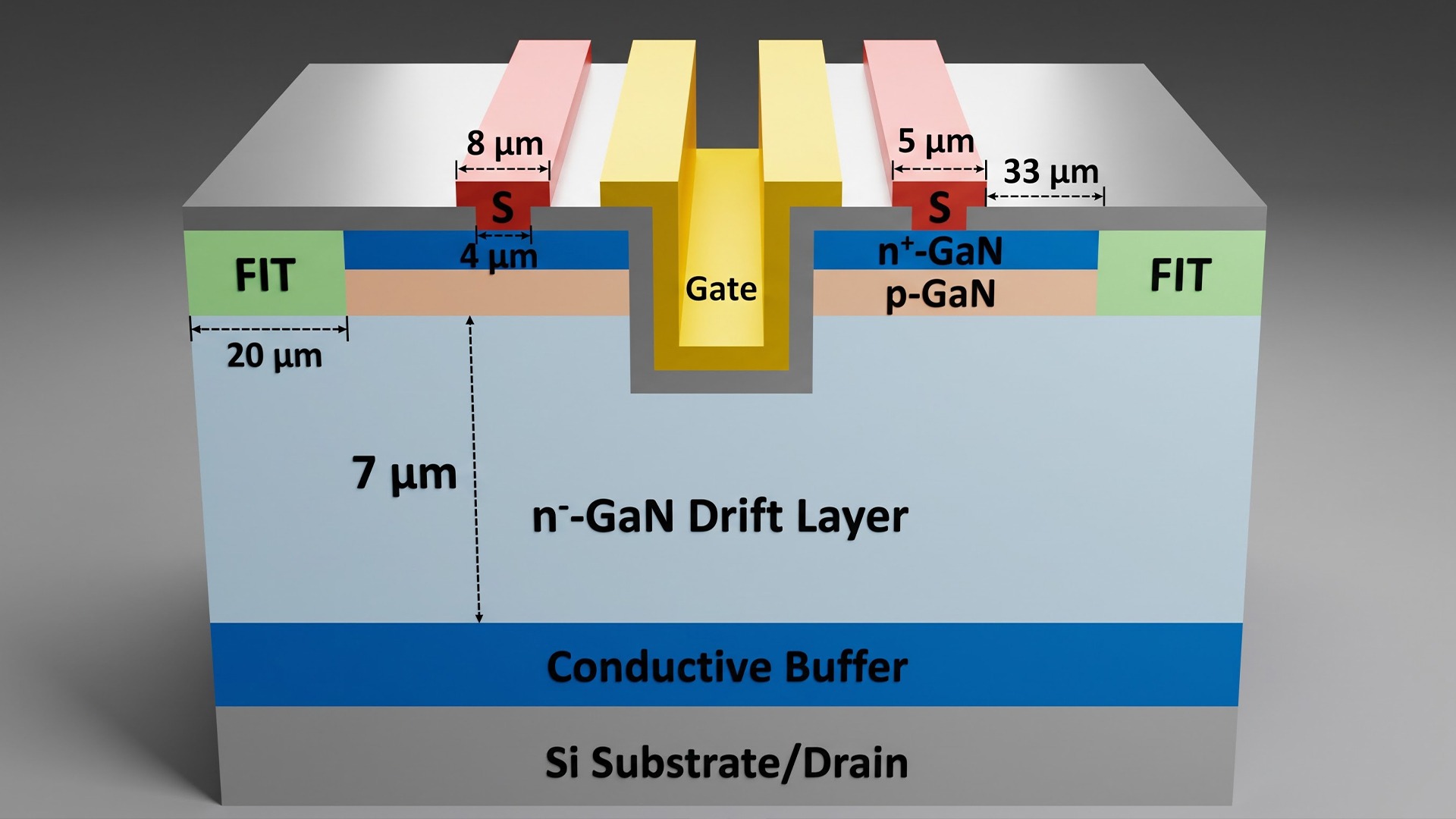
Over the past few decades, Si is the most widely used material for manufacturing GaN-based power devices especially for applications operating below 650 V. However, there are still differences between GaN and silicon that create challenges when it comes to material stress, cracking of wafer, defects and heat management.
Benefits of GaN-on-Si
a. Cost-Effective
GaN-on-Si is a primary commercial technology for cost-effective power electronics operating below 650V. The key reason for this lies in the substrate. Silicon wafers can be produced using standard silicon CMOS manufacturing facilities and in large diameter wafers. This helps in reducing production cost.
b. Easy to Scale
Silicon is available in large wafer diameters in 150mm, 200mm and even 300mm. A large sized silicon wafer basically means more dies can be achieved per run, thereby lowering the cost. GaN-on-Si can be produced using the existing established equipment rather than building dedicated lines. This manufacturing scalability, alongside raw wafer cost, is what makes GaN-on-Si the workhorse of high-volume power electronics.
Key Challenges
a. Material Mismatch
GaN and silicon have different crystal lattices along with different crystal structures. When combined, it creates defects at the interface. This affects the device performance, causes leakage, and affects reliability.
b. Wafer Stress
GaN and silicon also suffer from thermal stresses owing to the difference in the thermal expansion coefficient. The expansion of GaN and silicon is undertaken at different rates during the growth of GaN. Similarly after the growth is done, both the materials shrink unequally. This unequal dimensional change at a microscopic level leads to stress in the GaN layer. Furthermore, it also limits how thick the GaN layer can be grown and complicates downstream processing.
c. Thermal Limitations
Silicon has a low thermal conductivity of 150 W/m.K when compared with other materials including SiC and diamond. This makes it difficult to remove heat from GaN devices especially during continuous high-power operation. This is the reason why GaN-on-Si is best suited for moderate power applications and power switching.
GaN-on-SiC
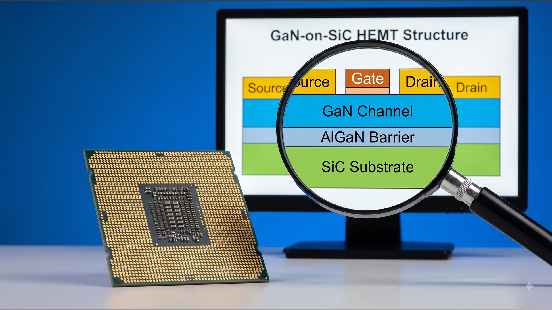
GaN-on-SiC is an advanced semiconductor technology wherein a thin layer of gallium nitride is grown on silicon carbide base. GaN when combined with SiC are wide bandgap semiconductors that bring the advantage of power efficiency, reduced cost and reduced size. Due to the higher output power applications, SiC has proven to be extremely valuable in the field of electric vehicles (EVs).
Additionally, GaN features higher switching frequency and lower power consumption. GaN and SiC have the potential to enhance the performance of power electronics and to get more effective outputs compared to traditional silicon devices.
Benefits
- GaN-on-SiC delivers higher power density, making them supremely valuable for the most demanding high-power applications.
- The high thermal conductivity of SiC draws heat away from the active device efficiently, supporting stable operation and long-term reliability.
- GaN-on-SiC features low switching and conduction losses. This reduces energy consumption and, in turn, operating costs.
- GaN’s fast electron transport and rapid switching capabilities enable operation at higher frequencies. This makes GaN-on-SiC well suited for multiple applications, where fast switching and signal processing are critical.
In short, GaN-on-SiC offers superior thermal management and high-power density. This makes it highly valuable in communication infrastructure that operates in the GHz switching realm.
Key Challenges
Though SiC and GaN offer several benefits, adopting them at a grand scale involves addressing multiple challenges. In this section, let us discuss in detail regarding the key challenges:
1. High Substrate Cost
The pricing of SiC is a major concern. The cost of the base layer equals almost half the cost of the whole device. It is far more difficult to produce SiC wafers than to produce silicon. Hence, GaN-on-SiC is ideal for applications where improving the performance is a top priority.
2. Size of the Wafer
Another challenge when it comes to GaN-on-SiC is the size factor. While silicon wafers can be grown in bigger sizes, growing SiC in bigger sizes is still a challenge. The demand for 150mm to 200mm is just beginning and this growing need requires advances in crystal growth, wafer polishing and defect reduction. A smaller size would mean few dies per run which will lead to higher cost per device.
3. Material Mismatch
SiC provides a better foundation for growing GaN than silicon because their crystal structures are more compatible. But this is still not a perfect match. There are additional layers required to control stress, reduce defects and electrically isolate the device. Hence, growing defect-free GaN might be difficult as these defects can affect the performance and reliability of the device.
GaN-on-Diamond
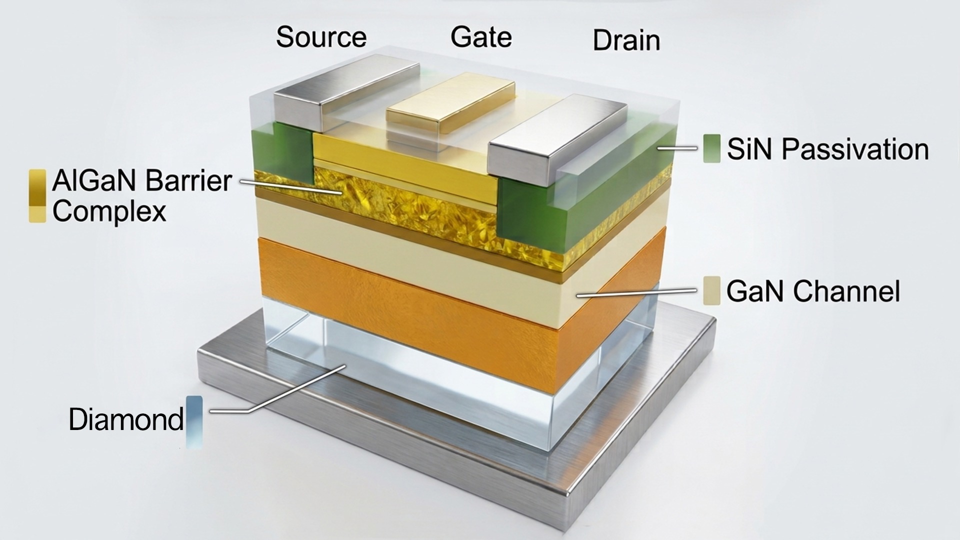
GaN-on-Diamond technology is emerging to be a key method for advancing next-generation power devices. Today, researchers and industry professionals are showing keen interest in GaN-on-Diamond technology as it can improve the performance and reliability of devices. It is emerging to be an advanced thermal management platform for high-power density RF devices.
Benefits
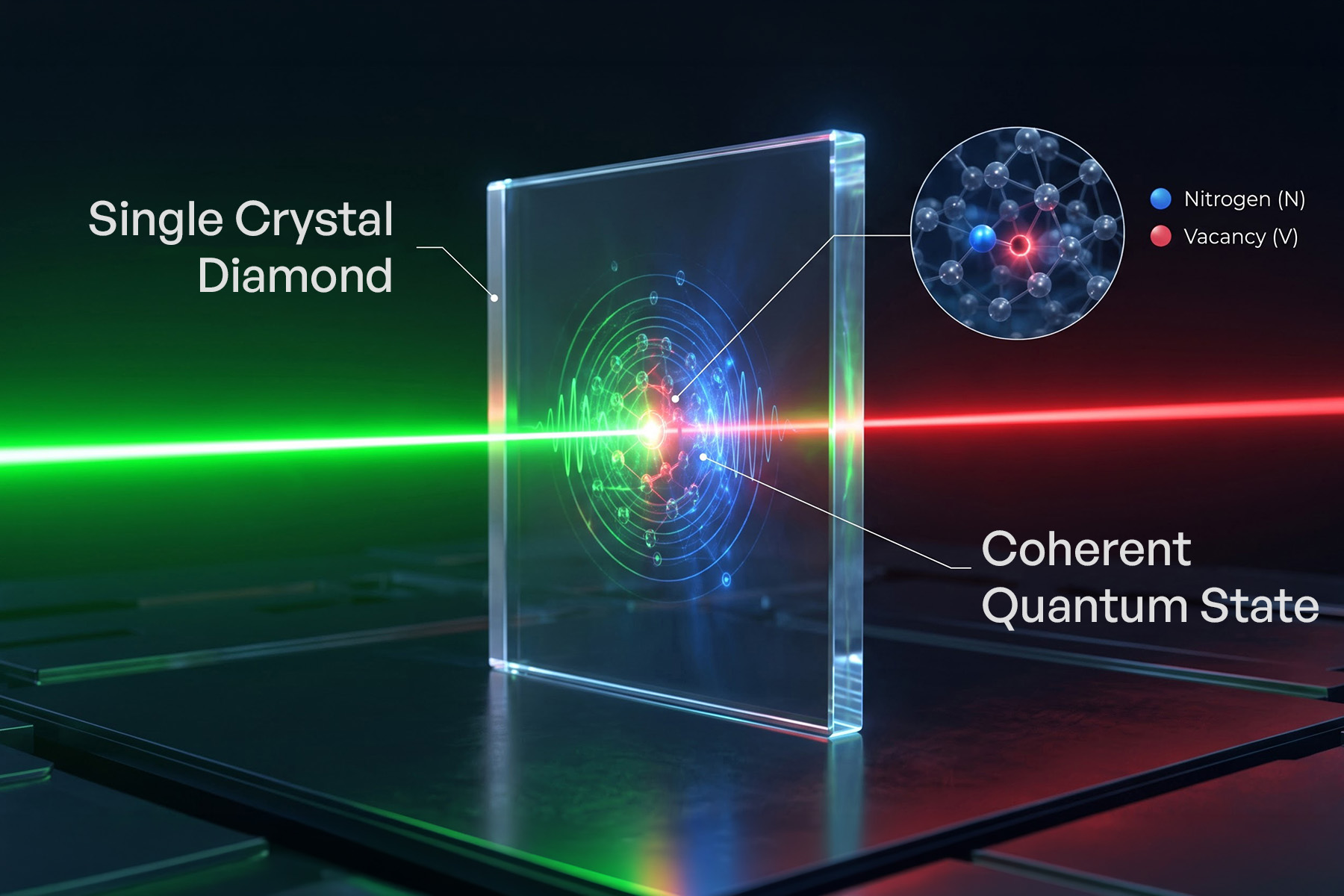
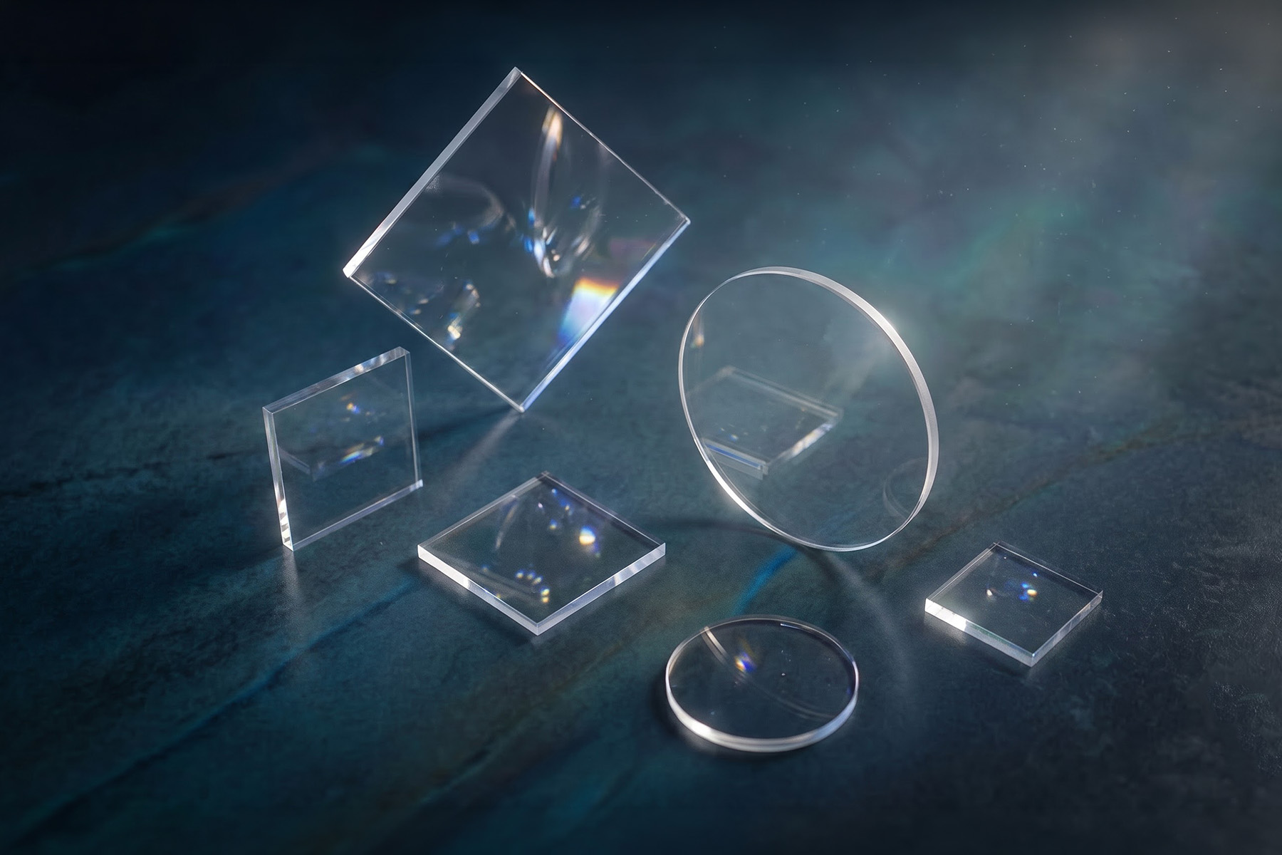
The thermal conductivity and thermal stability of GaN-on-Diamond makes them an excellent pick for heat and thermal management. The use of CVD diamonds as a substrate helps enhance the device performance by eliminating the self-heating issues. Some key advantages of CVD diamonds are as follows:
1. Better Heat Management
The thermal conductivity of diamond stands in the range of 1800 to 2200 W/m.K. This number is 10 times more than Si and 4 times more than SiC. The high thermal conductivity of diamonds can help prevent current collapse which is a state where GaN devices result in current drop under high-power operation. Hence, this makes GaN-on-Diamond a better substrate than GaN-on-Si and GaN-on-SiC.
2. Superior Mechanical Properties
The mechanical strength and thermal stability of CVD diamonds is far better than traditional materials. The hardness of diamonds can withstand mechanical stress, vibration and shock. Additionally, it also has low thermal expansion which helps prevent cracking when temperature changes.
3. Enhanced Performance
The high-power capability of GaN combined with diamond's exceptional thermal conductivity helps remove heat effectively. CVD diamonds help keep the devices cooler and allow GaN transistors to efficiently operate at higher power and frequency. This also results in higher power output from a small device and helps manufacturers develop more compact transmitters.
Key Challenges in Fabricating GaN-on-Diamond Wafers
There are certain challenges that are encountered while fabricating GaN-on-Diamond substrates. In this section, let us look at the different challenges:
1. Thermal Expansion Mismatch
The typical temperature required by CVD diamonds is >700 degrees C. Hence, during cool down, it creates thermal stress since at the interface both GaN and diamond expand and contract at different rates.
2. Wafer Cracking
Due to residual thermal stresses exceeding 1 GPa there are chances of severe wafer bowing, layer cracking and structural failure of epitaxial layers.
3. The Interface Bottleneck
The thermal boundary resistance between GaN and diamond is a key factor that holds performance below theoretical levels. Despite excellent bonding processes, the interface carries a thermal resistance of roughly 10 to 20 m²K/GW. This is enough to result in a meaningful temperature rise at extreme power densities.
GaN-on-Si vs GaN-on-SiC vs GaN-on-Diamond: Quick Comparison
The table below provides quick comparison between GaN-on-Si, GaN-on-SiC and GaN-on-Diamond:
Choosing the Right Substrate
In conclusion, choosing the right substrate is important and it will depend upon the specific application. The choice of the right substrate be it silicon (Si), silicon carbide (SiC), or diamond will affect how efficiently heat is removed, how well the materials work together, the device’s electrical performance, and the overall manufacturing cost. It will also depend upon a host of other factors including the target power density, thermal limitations and manufacturing budget.
GaN-on-Si is ideal for moderate power applications including consumer fast chargers, AC-DC/DC-DC power conversion, LED drivers, EV onboard chargers and lower-to-mid-power motor drives. GaN-on-SiC offers a good balance of thermal performance and power density for RF and EV systems. This includes high-power RF for defense, telecom infrastructure and satellite communications.
Finally, Gan-on-Diamond provides excellent heat dissipation for the most demanding high-power devices.
Frequently Asked Questions
Here are some interesting FAQs on GaN-on-Si vs GaN-on-SiC vs GaN-on-Diamond:
“redefining one diamond layer at a time”
More Articles


Aga9 Systems is a lab-grown diamond manufacturing company dedicated to harnessing the valuable properties of CVD diamonds for industrial applications. We at Aga9 Systems manufacture more than lab-grown diamond plates, we are dedicated to creating brilliance ethically, sustainably and with maximum resource efficiency.